ANNLab Virtual Semiconductor Cleanroom Training
6. Semiconductor Processing Laboratory Online Modules
A comprehensive 14-module journey from silicon crystal structure to advanced IC packaging, featuring interactive lab simulations, animated process visualizations, 51 self-assessment quiz questions, downloadable lecture notes, and a completion certificate.
👉 Click here to launch theSemiconductor Processing Laboratory Online Modules

5. Digital Twin Photolithography Training
Explore photolithography through an interactive digital twin simulation that replicates key steps of the semiconductor patterning process. This platform enables users to virtually perform critical stages such as resist coating, exposure, development, and pattern transfer, while observing how process parameters influence final feature quality. The simulation is designed to provide an intuitive and hands-on understanding of photolithography workflows, bridging theoretical concepts with practical process behavior in a controlled virtual environment. It is particularly suited for students, researchers, and trainees seeking to build foundational and applied knowledge in semiconductor fabrication. Created by Prof. Zafer Mutlu.
👉 Click here to launch the Digital Twin Photolithography Training:

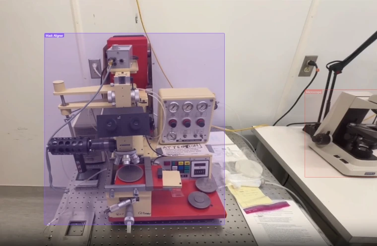
4. Cleanroom Virtual Reality (VR) Tour
Experience the University of Arizona’s cleanroom through an immersive virtual reality (VR) tour. This resource allows users to virtually explore the cleanroom environment, interact with key equipment areas, and gain a deeper understanding of cleanroom workflows and semiconductor fabrication processes. This resource was developed in close collaboration with Prof. Mehmet Belviranli’s team at the Colorado School of Mines, under the SMILE project, supported by the Microelectronics Commons Southwest Advanced Prototyping (SWAP) Hub. University of Arizona faculty involved in this project include Profs. Zafer Mutlu and Brian Kim.
👉 Click here to launch the Cleanroom VR Tour

3. Cleanrom Interactive Map
Navigate University of Arizona’s cleanroom through an interactive, Google Maps–style experience. This resource was developed in close collaboration with Prof. Mehmet Belviranli’s team at the Colorado School of Mines, under the SMILE project, supported by the Microelectronics Commons Southwest Advanced Prototyping (SWAP) Hub. University of Arizona faculty involved in this project include Profs. Zafer Mutlu and Brian Kim.
👉 Click here to open the Cleanroom Interactive Map

2. Cleanroom Interactive Video
Explore the University of Arizona cleanroom through an interactive video module that allows viewers to pause, click, and learn about key tools, processes, and workflows in semiconductor fabrication. This resource was developed in close collaboration with Prof. Mehmet Belviranli’s team at the Colorado School of Mines, under the SMILE project, supported by the Microelectronics Commons Southwest Advanced Prototyping (SWAP) Hub. University of Arizona faculty involved in this project include Profs. Zafer Mutlu and Brian Kim.
👉 Click here to open the Cleanroom Interactive Video
1. Cleanroom Video
Watch educational YouTube videos by the ANNLab team, covering semiconductor processing topics such as spin coating, lithography, atomic layer deposition, metrology, and more. This resource was developed for the SMILE project, supported by the Microelectronics Commons Southwest Advanced Prototyping (SWAP) Hub.
👉 Click here to open the Cleanroom Videos
